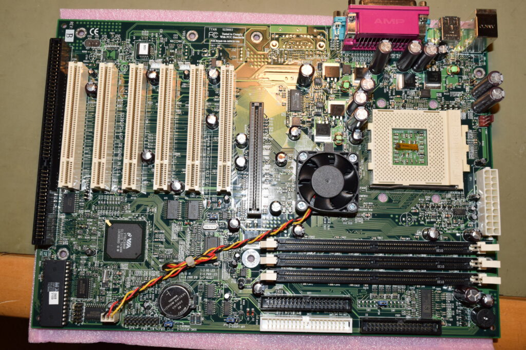
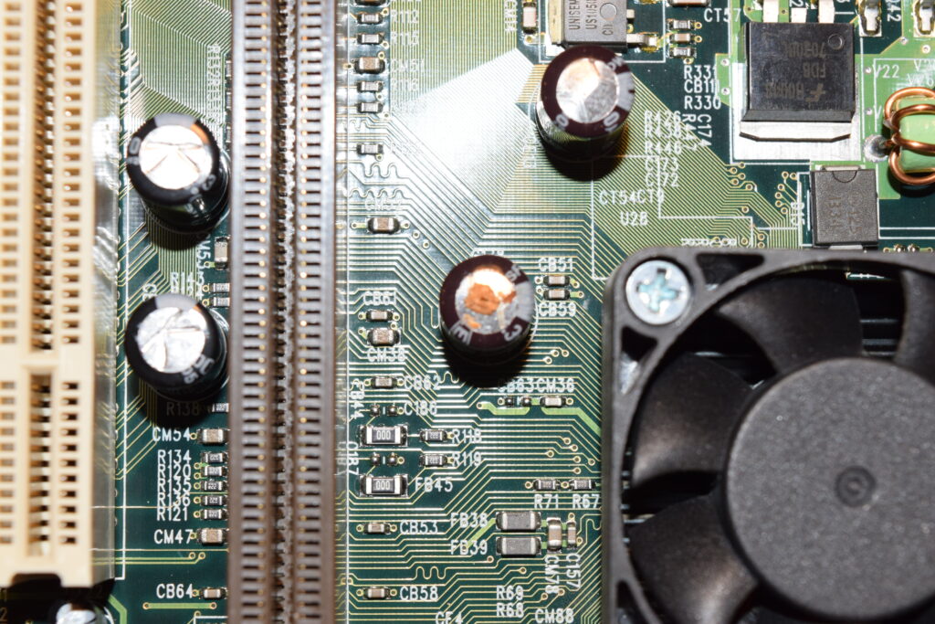
The conventional wisdom is that the bad capacitors (the ones with stolen chemical formula) bulged because of the hours you put in it. Today I found that it’s not true. I had a batch of new old stock Trinity S2390 motherboard (used in Agilent logic analyzers) and I noticed all the 100uF 6.3V capacitors bulged and one burst:
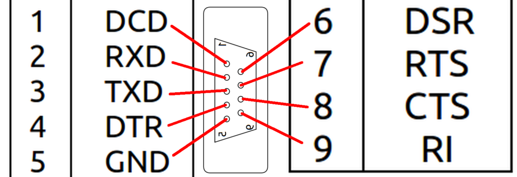
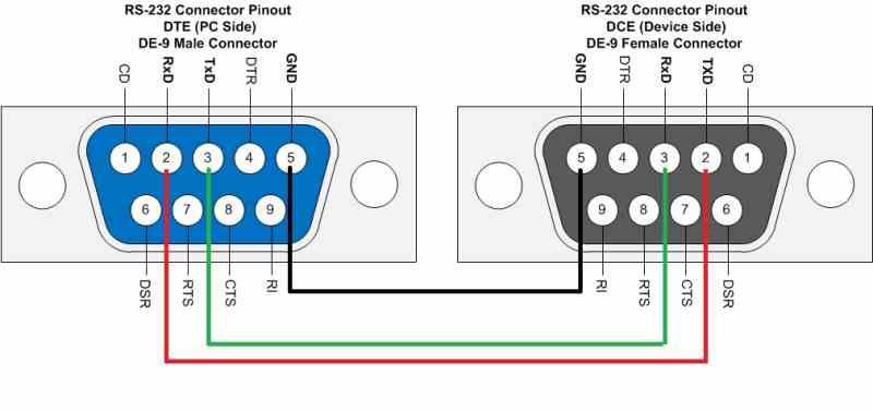
The pin ordering for RS-232 (DB9) pin is sequential is row-wise (the long side is a row) while the IDC-10 (ribbon cable) header is column-wise (zig-zag pattern).
This might be a little confusing because geometrically, they are in-place on both sides (you can overlay the pins of DB9 on top of IDC-10 and they align perfectly, except pin 6-9 was lowered by half a notch on the DB9 side). I am writing this post so nobody waste their time separating the wires in a ribbon just to find out the DB9 was designed so it aligns with the flat ribbon cable perfectly.
If you split the table on the right in half (cut after pin 5) and place pins 6 (DSR) ~ 9 (RI) on the right, you’ll see it align with the IDC10
1
DCD (Data Carrier Detect) Check if connection dropped
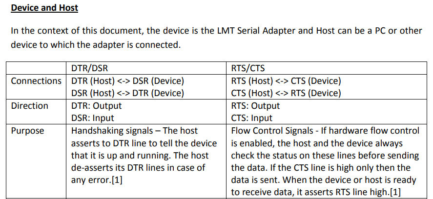
DSR (Data Set Ready) DTR-DSR Handshaking
6
2
RxD (Receive Data)
RTS (Request to Send) RTS-CTS Flow control
7
3
TxD (Transmit Data)
CTS (Clear to Send) RTS-CTS Flow control
8
4
DTR (Data Terminal Ready DTR-DSR Handshaking
RI (Ring Indicator) For phone rings
9
5
GND (Ground pin)
– (Not connected)
10
Rearranged DB9M RS-232 to align with IDC10
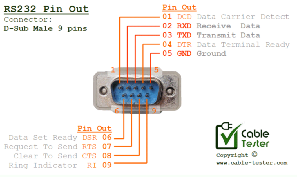
Cable-tester.com has a clearer annotated picture that matches the physical mapping above:
http://www.cable-tester.com/rs232-pin-out/
Note that the tutorial itself has Tx(D) and Rx(D) reserved it was building a null modem cable and they skipped all the handshake lines. I’m doing a straight cable (which should be done for internal board header cables where the DB9 socket is male, hence DB9M).
The DTE/DCE might be confusing. Hope these properties can help people make sense out of it (so you can figure it out in your head confidently instead of randomly trying null modem adapters till it work)
DTE device (colloquially ‘computer’) has the pattern as shown in the pictures above (receive pins above/before the transmit pins), which is usually the computer end and the port/socket is male. Think of it as the ‘driver/master’ (though it’s arbitrary)
DCE device (colloquially ‘modem’) reverses all the sends and receives of the DTE. Can think of it as the ‘receiver/slave’ (though it’s arbitrary). It’s usually the modem and the port/socket is female.
For DTE-DTE (like data transfer between two PCs), the send lines on one side should go to the receive lines on the other side. A null modem cable that swaps the send pins with receive pins. You can think of it as making one side DCE. Given that the topology is symmetric, it’s up to the software set up to decide which side is the initiator/client (master) and which side is the reactor/server (slave)
The handshaking (optional) and flow control (optional) lines also have their initiator/reactor roles reversed with null modem cable.
It turns out the direct geometric mapping (IDC male pins match the relative locations of the DB9 male pins) mentioned above is the less common type of motherboard header configuration. IDC ribbon crimp-on DB9 headers like this:
has to follow the above geometric layout since the pins cannot be remapped (so it has to follow the ribbon order). The soldered version looks like this:
https://store.cwc-group.com/lowprldb9mat1.html
However, the more commonly seen soldered RS-232M to IDC10 header uses a transposed configuration (which DB-9M pin numbers matches IDC-10 pin numbering EXACTLY despite one is row-major and the other is column-major), which has nothing to do with the IDC10 pin layout mentioned above.
https://store.cwc-group.com/lowprldb9mat.html (I don’t think it’s a good idea to call it ‘crossed-config’ like CWC did. It almost mislead me to think it happens to swap the roles of Tx and Rx. I did the mapping on paper and it didn’t make any sense. Let’s call it ‘transposed-configuration’)
The crazy thing about the existence of these 2 pin layouts is that there’s no easy way to tell which pin layout/mapping it is until you open the connector up and inspect the solder joints! Taking a pin and probe it with a multimeter is more work than taking the screw posts out and disassemble the connector.
So if you just buy some old scrap parts that came with old motherboards, this might confuse the heck out of you until you tested the pin mapping with a multimeter and realize things doesn’t add up!
Note to self: just open the DB9 side up whenever I see a DB9-IDC cable and mark the configuration on the DB9 end directly on the cable!
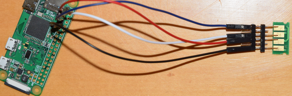
I am using a Raspberry Pi Zero W so the chip is BCM2835 instead and I can use 100Kbps/400KBps instead of 9600 baud as in the original code
The electrical pins we need is clustered on to top left, Pins 1 (3.3V), 3 (I2C SDATA), 5 (I2C SCLK), 9 (Ground)
While looking for the pinouts (https://pinout.xyz/pinout/i2c), I discovered a useful tool called i2cdetect that allows me to find out the address of the chips which means I can write a program automatically figure out the right image to load to the chip without looking:
Sorry I forgot where I got this image from. Please remind me in the comments section if you find out who should I credit it to.
Since I don’t have cheap pogo pins lying around, I took the 2.4mm pitch (the standard size used in PC, Arduino and Raspberry Pi) jumper block I have (so all pins are set at equal lengths to make simultaneous contact) and hope somehow there’s 4 pins that kind of align with the contact, and it did. See pictures here:
Can press the pins down by using jumpers
You might be worried about shorting into the next pin or hooking something up in reverse damaging the chips, but luckily the chips survived. My guess is that it’s a good design to put the Vcc next to Ground on one side instead of making it symmetric so the polarity can be reversed. When reversed, SCL is set to low (Ground), SDA is pulled up to Vcc while there is no power supply, so no damage is done. Brilliant! The worst case for my poorly aligned jumper block is that SDA and Vcc might touch each other, but it doesn’t matter because it’s a perfectly legal hookup (just not communicating)!
So no worries if you didn’t touch the pins right! The only case it might go wrong is if you intentionally flip the block and slide it by two pins (reversing Vcc and Ground). Other cases (you are likely going to run into) are pretty much data lines getting hooked high or low levels while power lines not getting any supplies.
I’ve designed the program that it’ll detect the chip if you hook it up right and immediately program the chip (takes only a second), so you don’t have to hold the jumper for too long to worry about unstable contacts.
#!/bin/bash

# This program detects rewrite the toner chips to "full" for a Ricoh SP C250SF/DN Printer using Raspberry PI (defaults to BCM2835 models such as Raspberry PI Zero)

# The chip data is in file named "black" "cyan" "magenta" and "yellow".
# The pad closest to the edge is GND (-> Pin 9), followed by VCC (-> Pin 1) , DATA (-> Pin 3), and Clock (-> Pin 5).

# Be sure i2c is enabled and installed (it's turned off by default) on Raspbian

# This line is disabled because it takes too long to unregister i2c_bcm2835 to start from a clean slate
# modprobe -r i2c_bcm2835

# This program needs sudo permissions as it involves direct access to hardware
if [[ $EUID -ne 0 ]]; then
  echo "Need root permissions as this code involves direct hardware access. Try sudo"
  exit 2
fi

# Sets the baud rate
modprobe i2c_bcm2835 baudrate=400000

# Install i2cdetect if not exist (This idiom uses short-circuit OR for conditional exec)
command -v i2cdetect > /dev/null 2>&1 || {sudo apt-get install i2c-tools}

# Create I2C address to color map
COLORS=( [50]="yellow" [51]="magenta" [52]="cyan" [53]="black" )
# Detect chip I2C address
I2C_address=$( sudo i2cdetect -y 1 | grep 50 | sed -e 's/50: //;s/-- //g' )
# Keep the 0x5* address lines since only 0x50~0x53 is valid. Strip the 50: header, discard all "--" entries, and you are left with the detected address
HEX_I2C_address="0x$I2C_address"

# LED flash function(s)
target_device="/sys/class/leds/led0/brightness"
# This accounts for breaking changes (by renaming led0 to ACT) from Bookworm
[ -f ${target_device} ] || target_device="/sys/class/leds/ACT/brightness"

function turn_off {
  echo 0 > ${target_device}
}
function turn_on {
  echo 1 > ${target_device}
}
function toggle {
  # PI Zero only has 1 power LED which is on/off
  # Reads 0 for OFF and 255 for ON
  readin=$(cat ${target_device})
  # Condition 255 to 1 to reduce platform dependency
  state=$[$readin>0]
  # Not equal to 1 is XOR (flip)
  flip=$[$state != 1]
  # Display output
  echo $flip > ${target_device}
}

function flash_once {
  period=${1:-0.5}

  toggle
  sleep $period

  toggle
  sleep $period
}

function flash {
  times=${1:-1}
  period=$2
  for((i=1; i<=times; i++)); do
    flash_once $period
  done
}

echo "Detecting toner chip ..."
turn_off
if [ -v COLORS[I2C_address] ]; then
  # Meat
  color=${COLORS[I2C_address]}
  echo "Detected toner chip for color: $color"

   # "address" counter sync up with the hex code index in file
   printf "Writing"
   address=0;
   datafile="${BASH_SOURCE%/*}/${color}"
   for i in $(cat $datafile); do
     i2cset -y 1 ${HEX_I2C_address} $address $i; || break
     address=$(($address +1));
     printf .
     flash 1 0
   done
   echo "Done!"
   turn_on
else
  echo "Invalid I2C address for SP C250DN/SF toner chips. ${I2C_address}"
  turn_on
  exit 4
fi
Turns out Linux’s dot sourcing (bash calling) syntax is relative to your current folder, not the scripts’ folder. So if you have one script calling another in the same folder when you are not currently at the same folder as the script (e.g. startup automation), the relative paths will be wrong. So instead of ./ , you should use this prefix instead:
${BASH_SOURCE%/*}/
I chose to flash the board’s only LED light quickly before starting and blink slowly a few times after it’s done for visual clues. It’s entirely optional. Here’s the guts of the code without the fancy indicators:
#!/bin/bash

# Sets the baud rate
modprobe i2c_bcm2835 baudrate=400000

# Create I2C address to color map
# Note that the dictionary/hash keys below are abusively pretending the hex are decimals
# since the i2cdetect()'s output is text showing hex values without the "0x" prefix
# I got away with this because the only 4 possible choices are 0x50 .. 0x53
# so I never ran into 'A...F'. Do not imitate this. The output of i2cdetect()
# is already messy to parse so it'd make the code complicated to keep track of hex.
COLORS=( [50]="yellow" [51]="magenta" [52]="cyan" [53]="black" )

# Detect chip I2C address
I2C_address=$( sudo i2cdetect -y 1 | grep 50 | sed -e 's/50: //;s/-- //g' )
HEX_I2C_address="0x$I2C_address"

if [ -v COLORS[I2C_address] ]; then
  # Meat
  color=${COLORS[I2C_address]}

  # "address" counter sync up with the hex code index in file
  address=0;
  for i in $(cat ${color}); do
    i2cset -y 1 ${HEX_I2C_address} $address $i || break
    address=$(($address +1));
  done
else
  echo "Invalid I2C address for SP C250DN/SF toner chips: ${I2C_address}"
fi
This downloadable is old and might not reflect the update directly improvements directly reflected on the blog page’s code listing. I’ll get to it when I have some time.
Just in case if people are wondering. The L01 chip’s datasheet is here:
To make a dedicated Raspberry Pi Zero device to run this script (program_toner) repeatedly on boot, I made a script loop_program_toner that runs the same program as infinite loop.
Since writing starts immediately once the chip is identified (no reason to hold the pogo pins for longer than needed), once the chip is detected, whether the writing finished successfully or not, threre’d be 5 seconds of delay so you can reseat the pogo pins (on write failure) or remove the pogo pins (so it won’t unnecessarily rewrite the chip again).
#!/bin/bash

if [[ $EUID -ne 0 ]]; then
  echo "Needs root permissions. Try sudo"
  exit -2
fi

while :
do
  bash "${BASH_SOURCE%/*}/program_toner"
  if (($?)); then
    # Wait longer to give time to detatch probe once chip is detected
    # whether the process completed successfully or not
    sleep 5;
  else
    sleep 1;
  fi
done
There are a few steps needs to auto make this automated:
Have a user account dedicate to autorun the program on boot. In the example here, we’ll use Raspberry Pi’s default admin account
Auto-logged on by running sudo raspi-config, select (1) System Option > (S5) Boot / Auto Login > (B2) Console Autologin
Bless the said account with password free sudo rights: Run sudo visudo and add this to the end (replace admin with something else if you chose a different username)
admin ALL=(ALL) NOPASSWD:ALL
Call loop_program_toner in ./profile or ~/.bashrc (startup script). Can place this at the bottom if your package folder is ~/spc250dn :
sudo ./spc250dn/loop_program_toner
The path can start with . or ~ because you are starting with at home folder anyway.
Do they have an idea how many code they’ll break and how many man hours they will waste the world to discover this breaking change when updating the distro? Non-caught exceptions just fall through and shows up as mysterious error messages!
If you want people to get the memo and change their code to match a more sensible notation, feel free to put in a warning stub, but hell no to just flip a switch and watch the world scream! This is apparently not a difficult decision to make when adding backward compatibility would be a huge project because of some catch-22 conditions!
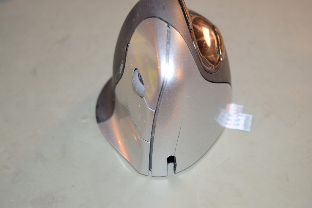
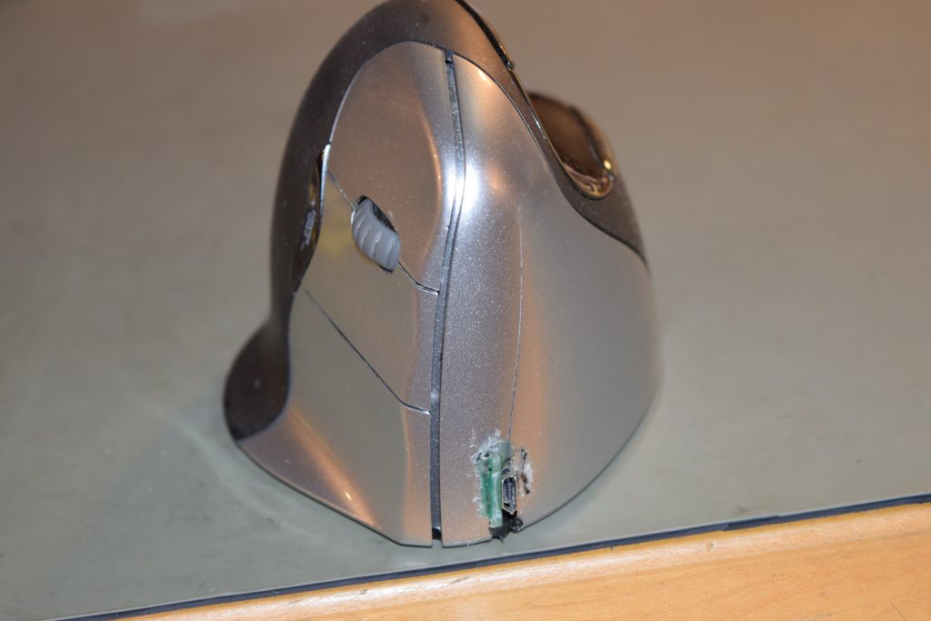
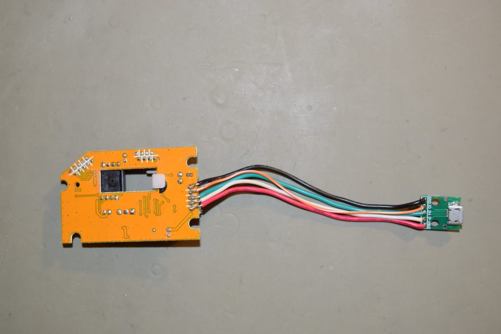
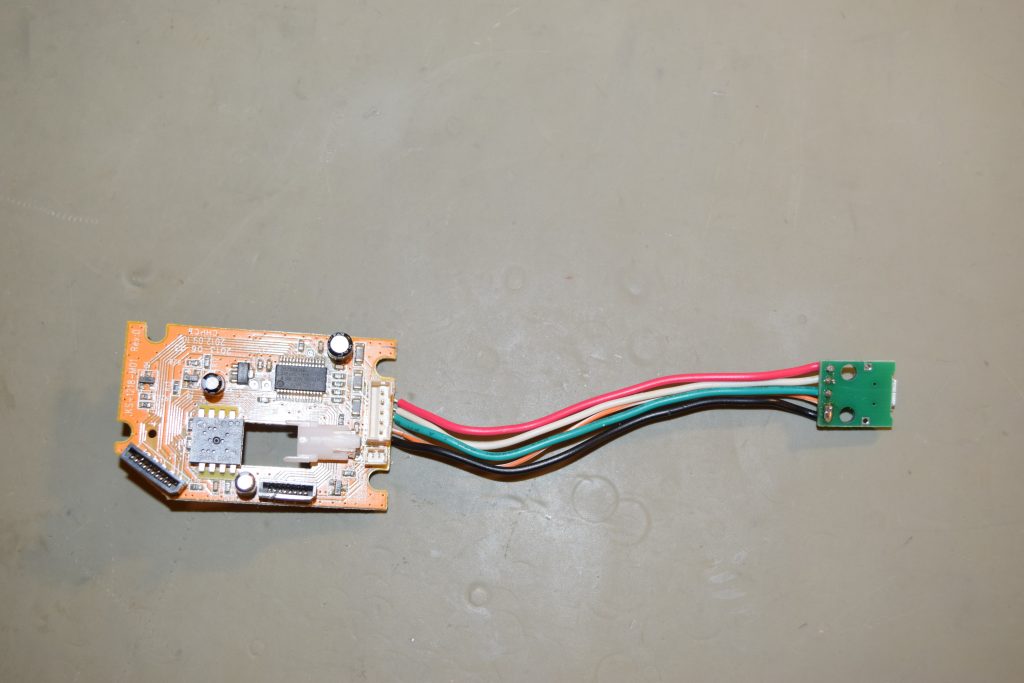
The mouse cable for Evoluent Vertical Mouse 4 is extremely long, which creates a lot of clutters especially when my keyboard has a USB hub relay built in (it’s the mouse is less than a feet away from it). Instead of splicing the cable, which creates a hard junction that’s not flexible, I modified the mouse to take a micro-USB cable instead.
While clearing out my old data, I came across the teaching materials I’ve helped rewritten as a teaching assistant of Biomedical Electronics Lab (Stanford EE122A).
It’s a generic concept in electronics that often used in EKG/ECG circuits to remove the baseline drift on the fly so the analog signal won’t drift off the rails (exceed the dynamic range limited by the op-amps) before the post-processing filter (whether it’s analog or digital) kicks in to remove the DC component.
This concept is called ‘DC restoration’, which is often not taught in standard electronics textbooks. Instead it’s detailed in one of the instrumentation amp (INA) Burr-Brown (now TI) application notes.
It’s a slick trick but the rationale wasn’t very well explained even in the application note itself. It was presented as a feedback design but it doesn’t tell you intuitively what was fed back and why the reference pin is the right injection point.
Most textbooks don’t even teach the existence of the reference pin (they always short the reference to the ground without explaining). Application notes talk about the REF pin, but they often jump too quickly into cookbook recipes and equations (likely because customers just want quick answers) so they never tell you the thought process.
This blog post shares my intuition of DC-restoration shared with EE122A students through updating their first generation lab document (written by the last TA). Hope electronic hobbyists and industry people will find it useful.
Before we get to DC restoration, we must see that the purpose of a 3-amp INA is basically a non-inverting buffer (often plus gain) stage (primarily done to increase input impedance) followed by a single (often unity) difference amp (output) stage.
Non-inverting configuration has higher input impedance as the input goes directly to the high impedance non-inverting (+) input pin without taking material current from the input (loading), so there’s no good reason to lose this property by doing inverting op-amp configuration twice.
Most practical INA chips assign some of the user-adjustable gains at the buffer stage because ‘mirrored-ground’ ( is the superposition of two different by shorting the other input to ground one at a time) allows one resistor to program the gains for the 2 buffer amps without adding more mismatch, but conceptually the first stage’s primary purpose is a buffer. The rest of the gains can be hard-coded by manufacturing with matched ‘resistors’ inside the IC, mostly at the output difference amp stage.
But for illustration (so not to drown the readers in math), let’s assume the design choice of assigning the gains at the input buffer stage and make the output stage a unity gain difference amplifier (–), which I use small letters (, ) to denote the outputs of the buffer stage internal to the INA chip.
https://www.ti.com/lit/an/sboa003/sboa003.pdf
The REF pin (the part of exposed in Figure 6 above) is often advertised as an offset adjustment pin. This is just one of the many uses if you really understand the idea behind the 1-amp difference amplifier configuration.
The slightly more shallow perspective (more modular or system perspective that I’ve shared with EE122A students) is that if you look at an standard 3-amp INA configuration in regular textbooks like this,
the entire sub-circuit (3 amp INA) is floating so it has absolutely no idea what the reference (‘ground’) would have been if we did not ARBITRARILY define it through by tying it to the CM ground, by forcing REF pin () to be 0V (relative to the common mode ground shared with the inputs)!
In other words, we now have an INA ‘ground’ and a Common Mode (CM) ground, which they do not have to be the same unless we force them to be equal by shorting the REF pin to the CM ground.
This means whatever voltage we set the REF pin to be, it’s the baseline of the system (amplifier) and the whole output shifts moves up and down by whatever relative to common mode ground we are feeding into the REF pin for the moment.
The DC restoration takes advantage of the user-definable baseline (INA ‘ground’) by extracting a low-frequency (drift) portion of the output signal with an INVERTING low-pass filter (LPF) with frequency response , and re-define it as the INA’s ‘ground’ level. This is the LPF:
e.g. if the signal’s baseline drifted up by 1V, a -1V is generated by the inverting LPF and the INA ‘ground’ respond by moving from 0V down to -1V, which pulls the entire signal down by 1V, cancelling the 1V increase in baseline. All the voltages used here are relative to the common mode ground.
As with any AC coupling circuit, there is no precise definition of what ‘DC’ or ‘baseline’ is. It’s up to the experimenter to consider what cutoff frequency in the LPF is close enough.
The feedback (how fast the INA ‘ground’ is readjusted) is as responsive as the phase delay introduced by the LPF’s time constant. If you only consider anything below 0.00001Hz to be DC, you have to pay a price for the long delay catching up to the changes which might or might not be considered a baseline drift (it’s an application specific context).
Technically you can replace the feedback signal manipulation with DSP doing running window of trimmed-median to derive a baseline instead of the inverting analog DC extractor above if you are willing to deal with complexity of mixed signals.
DC restoration is merely counteracting the baseline drifts with the ‘baseline’ your feedback (DC extractor) algorithm/mechanism observed/derived from the output signal almost instantly. If your feedback block delays the baseline observation, there’d be a lag catching up to the baseline drifts.
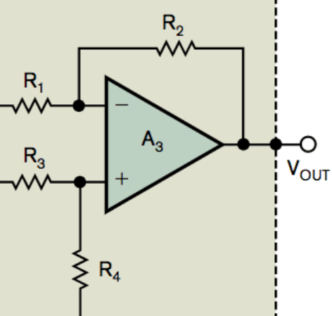
I also have an alternate view of DC restoration which does not use the concept of INA ‘ground’ (not taught in EE122A). This is based on seeing the final stage op-amp (1-amp INA) not just as a simple difference amplifier, but as a 3-input arithmetic circuit (summing and subtractions) through super-position (setting one input to 0V at a time and add the results up).
This is the gut of a 1-amp INA difference amplifier
We can break it down into a (1 input) inverting amplifier plus a summing (2 inputs) non-inverting amplifier.
The equations for inverting amplifier and non-inverting amplifiers are not symmetric! The feedback gain in EITHER CONFIGURATION are ALWAYS set at the feedback branch which ONLY goes to the inverting input (-), aka and !
The inverting amplifier portion (top half) do not care about the resistors at the non-inverting input (+), but
The non-inverting amplifier portion’s (lower half) gain is determined by the 2 resistors at the inverting input (-)!
Resistors at the non-inverting inputs (+) never boost the amplifier gains! They only attenuate signal from external sources (like voltage dividers). The gain boost happens ONLY at the inverting branch!
Why? By superposition (short out other inputs you are not considering)
Inputs to () and () shorted to the common ground gives an inverting amplifier. They don’t matter to . The gain to is .
Input to () shorted to the common ground gives a non-inverting amplifier, which the gain boost () is relative to voltage showing up at the non-inverting input (+).
is the result of attenuating through and attenuating through added together.
The output contributions, if and ,
[Inverting amplifier gain of -1 relative to ] contributes to the output
[Non-inverting amplifier gain of 2 relative to ] if is set to ground through .
and forms a 1:1 potential divider which halves to give at .
Doubling (2x gain) the halved input gives an overall gain of 1, therefore contributing to the output
So the overall output equation is if is grounded to 0V.
The intuition for DC restoration is to untie the REF pin (going to ) from CM ground and treat it as equals to pin (going through , so instead of a potential divider, they form a non-inverting summing amplifier:
So the DC restoration circuit can be seen as a 3-input arithmetic amplifier that gives the equation and you can subtract the baseline by setting to be whatever baseline your inverting LPF feedback branch judged. The overall AC-coupled system response is .
Note that ALL 3 inputs () should be driven from sources with low output impedance. and is the outputs of a buffer op-amp so they already have good low impedance outputs feeding to the last stage. We’ll need to do the same for by using an op-amp to lower the output resistance whether it is an active low pass filter or active potential divider, because do not see differently from . Noise showing up from high resistance output driving REF pin do not simultaneously appear on , so it’s not canceled and therefore it’s worsening the common mode rejection (CMR).


![ฅนบ้ายอ: [34+] Db9 Male And Female Connector Pinout](https://external-content.duckduckgo.com/iu/?u=https%3A%2F%2Fsharvielectronics.com%2Fwp-content%2Fuploads%2F2020%2F09%2FD-SUB-DB9-9-Pin-Male-Connector-To-IDC-Female-10-Pin-Flat-Cable-30CM_1.jpg&f=1&nofb=1)

 is the superposition of two different
  by shorting the other input to ground one at a time) allows one resistor to program the gains for the 2 buffer amps without adding more mismatch, but conceptually the first stage’s primary purpose is a buffer. The rest of the gains can be hard-coded by manufacturing with matched ‘resistors’ inside the IC, mostly at the output difference amp stage.
 –
– ), which I use small letters (
 ,
,  ) to denote the outputs of the buffer stage internal to the INA chip.
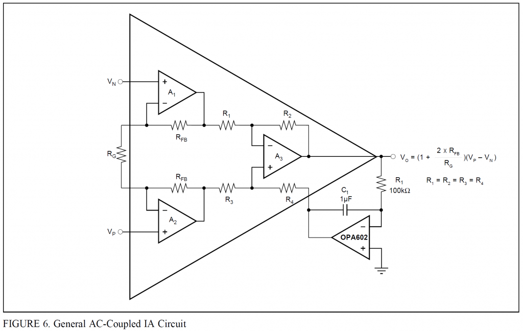
 exposed in Figure 6 above) is often advertised as an offset adjustment pin. This is just one of the many uses if you really understand the idea behind the 1-amp difference amplifier configuration.
 ) to be 0V (relative to the common mode ground shared with the inputs)!
  with an INVERTING low-pass filter (LPF) with frequency response
  , and re-define it as the INA’s ‘ground’ level. This is the LPF:
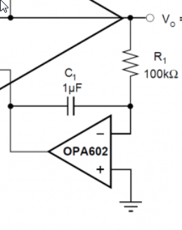
 and
and  !
! (
( .
. ) is relative to voltage
  showing up at the non-inverting input (+).
  and
and  ,
, to the output
 at
at  if
if 
 and you can subtract the baseline by setting
  .
. ) should be driven from sources with