While clearing out my old data, I came across the teaching materials I’ve helped rewritten as a teaching assistant of Biomedical Electronics Lab (Stanford EE122A).
It’s a generic concept in electronics that often used in EKG/ECG circuits to remove the baseline drift on the fly so the analog signal won’t drift off the rails (exceed the dynamic range limited by the op-amps) before the post-processing filter (whether it’s analog or digital) kicks in to remove the DC component.
This concept is called ‘DC restoration’, which is often not taught in standard electronics textbooks. Instead it’s detailed in one of the instrumentation amp (INA) Burr-Brown (now TI) application notes.
It’s a slick trick but the rationale wasn’t very well explained even in the application note itself. It was presented as a feedback design but it doesn’t tell you intuitively what was fed back and why the reference pin is the right injection point.
Most textbooks don’t even teach the existence of the reference pin (they always short the reference to the ground without explaining). Application notes talk about the REF pin, but they often jump too quickly into cookbook recipes and equations (likely because customers just want quick answers) so they never tell you the thought process.
This blog post shares my intuition of DC-restoration shared with EE122A students through updating their first generation lab document (written by the last TA). Hope electronic hobbyists and industry people will find it useful.
Before we get to DC restoration, we must see that the purpose of a 3-amp INA is basically a non-inverting buffer (often plus gain) stage (primarily done to increase input impedance) followed by a single (often unity) difference amp (output) stage.
Non-inverting configuration has higher input impedance as the input goes directly to the high impedance non-inverting (+) input pin without taking material current from the input (loading), so there’s no good reason to lose this property by doing inverting op-amp configuration twice.
Most practical INA chips assign some of the user-adjustable gains at the buffer stage because ‘mirrored-ground’ ( is the superposition of two different
  by shorting the other input to ground one at a time) allows one resistor to program the gains for the 2 buffer amps without adding more mismatch, but conceptually the first stage’s primary purpose is a buffer. The rest of the gains can be hard-coded by manufacturing with matched ‘resistors’ inside the IC, mostly at the output difference amp stage.
But for illustration (so not to drown the readers in math), let’s assume the design choice of assigning the gains at the input buffer stage and make the output stage a unity gain difference amplifier ( –
– ), which I use small letters (
 ,
,  ) to denote the outputs of the buffer stage internal to the INA chip.
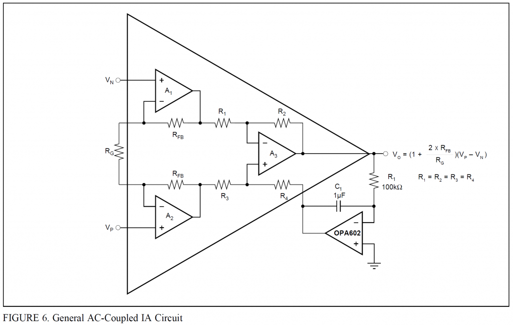
The REF pin (the part of  exposed in Figure 6 above) is often advertised as an offset adjustment pin. This is just one of the many uses if you really understand the idea behind the 1-amp difference amplifier configuration.
The slightly more shallow perspective (more modular or system perspective that I’ve shared with EE122A students) is that if you look at an standard 3-amp INA configuration in regular textbooks like this,

the entire sub-circuit (3 amp INA) is floating so it has absolutely no idea what the reference (‘ground’) would have been if we did not ARBITRARILY define it through by tying it to the CM ground, by forcing REF pin ( ) to be 0V (relative to the common mode ground shared with the inputs)!
In other words, we now have an INA ‘ground’ and a Common Mode (CM) ground, which they do not have to be the same unless we force them to be equal by shorting the REF pin to the CM ground.
This means whatever voltage we set the REF pin to be, it’s the baseline of the system (amplifier) and the whole output shifts moves up and down by whatever relative to common mode ground we are feeding into the REF pin for the moment.
The DC restoration takes advantage of the user-definable baseline (INA ‘ground’) by extracting a low-frequency (drift) portion of the output signal  with an INVERTING low-pass filter (LPF) with frequency response
  , and re-define it as the INA’s ‘ground’ level. This is the LPF:
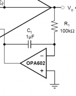
e.g. if the signal’s baseline drifted up by 1V, a -1V is generated by the inverting LPF and the INA ‘ground’ respond by moving from 0V down to -1V, which pulls the entire signal down by 1V, cancelling the 1V increase in baseline. All the voltages used here are relative to the common mode ground.
As with any AC coupling circuit, there is no precise definition of what ‘DC’ or ‘baseline’ is. It’s up to the experimenter to consider what cutoff frequency in the LPF is close enough.
The feedback (how fast the INA ‘ground’ is readjusted) is as responsive as the phase delay introduced by the LPF’s time constant. If you only consider anything below 0.00001Hz to be DC, you have to pay a price for the long delay catching up to the changes which might or might not be considered a baseline drift (it’s an application specific context).
Technically you can replace the feedback signal manipulation with DSP doing running window of trimmed-median to derive a baseline instead of the inverting analog DC extractor above if you are willing to deal with complexity of mixed signals.
DC restoration is merely counteracting the baseline drifts with the ‘baseline’ your feedback (DC extractor) algorithm/mechanism observed/derived from the output signal almost instantly. If your feedback block delays the baseline observation, there’d be a lag catching up to the baseline drifts.
I also have an alternate view of DC restoration which does not use the concept of INA ‘ground’ (not taught in EE122A). This is based on seeing the final stage op-amp (1-amp INA) not just as a simple difference amplifier, but as a 3-input arithmetic circuit (summing and subtractions) through super-position (setting one input to 0V at a time and add the results up).
This is the gut of a 1-amp INA difference amplifier
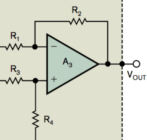
We can break it down into a (1 input) inverting amplifier plus a summing (2 inputs) non-inverting amplifier.
The equations for inverting amplifier and non-inverting amplifiers are not symmetric! The feedback gain in EITHER CONFIGURATION are ALWAYS set at the feedback branch which ONLY goes to the inverting input (-), aka  and
and  !
!
- The inverting amplifier portion (top half) do not care about the resistors at the non-inverting input (+), but
- The non-inverting amplifier portion’s (lower half) gain is determined by the 2 resistors at the inverting input (-)!
Resistors at the non-inverting inputs (+) never boost the amplifier gains! They only attenuate signal from external sources (like voltage dividers). The gain boost happens ONLY at the inverting branch!
Why? By superposition (short out other inputs you are not considering)
- Inputs to
 () and () shorted to the common ground gives an inverting amplifier. They don’t matter to . The gain to is
  .
. - Input to () shorted to the common ground gives a non-inverting amplifier, which the gain boost (
 ) is relative to voltage
  showing up at the non-inverting input (+). is the result of attenuating through and attenuating through added together.
The output contributions, if  and
and  ,
,
- [Inverting amplifier gain of -1 relative to ] contributes
 to the output
 - [Non-inverting amplifier gain of 2 relative to ] if is set to ground through . and forms a 1:1 potential divider which halves to give
 at .
at .
Doubling (2x gain) the halved input gives an overall gain of 1, therefore contributing to the output
So the overall output equation is  if is grounded to 0V.
The intuition for DC restoration is to untie the REF pin (going to ) from CM ground and treat it as equals to pin (going through , so instead of a potential divider, they form a non-inverting summing amplifier:
So the DC restoration circuit can be seen as a 3-input arithmetic amplifier that gives the equation  and you can subtract the baseline by setting to be whatever baseline your inverting LPF feedback branch judged. The overall AC-coupled system response is
  .
.
Note that ALL 3 inputs ( ) should be driven from sources with low output impedance. and is the outputs of a buffer op-amp so they already have good low impedance outputs feeding to the last stage. We’ll need to do the same for by using an op-amp to lower the output resistance whether it is an active low pass filter or active potential divider, because do not see differently from . Noise showing up from high resistance output driving REF pin do not simultaneously appear on , so it’s not canceled and therefore it’s worsening the common mode rejection (CMR).
![]()