The pin ordering for RS-232 (DB9) pin is sequential is row-wise (the long side is a row) while the IDC-10 (ribbon cable) header is column-wise (zig-zag pattern).
This might be a little confusing because geometrically, they are in-place on both sides (you can overlay the pins of DB9 on top of IDC-10 and they align perfectly, except pin 6-9 was lowered by half a notch on the DB9 side). I am writing this post so nobody waste their time separating the wires in a ribbon just to find out the DB9 was designed so it aligns with the flat ribbon cable perfectly.
Here’s a great tutorial building your own RS-232 cable which I took the images from to illustrate the point. Please pay them a visit to show some love: https://developer.toradex.com/knowledge-base/assembling-serial-idc-to-db9-cable

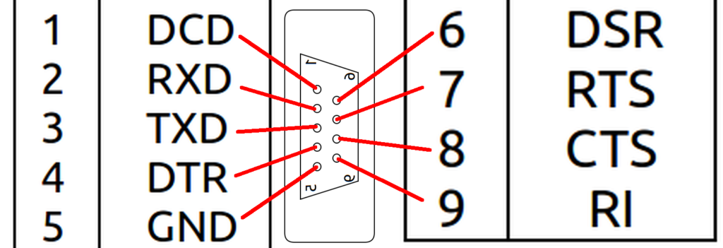
IDC10 RS-232
(Motherboard male pins perspective)
DB9M RS-232
If you split the table on the right in half (cut after pin 5) and place pins 6 (DSR) ~ 9 (RI) on the right, you’ll see it align with the IDC10
| 1 | DCD (Data Carrier Detect) Check if connection dropped | DSR (Data Set Ready) DTR-DSR Handshaking | 6 |
| 2 | RxD (Receive Data) | RTS (Request to Send) RTS-CTS Flow control | 7 |
| 3 | TxD (Transmit Data) | CTS (Clear to Send) RTS-CTS Flow control | 8 |
| 4 | DTR (Data Terminal Ready DTR-DSR Handshaking | RI (Ring Indicator) For phone rings | 9 |
| 5 | GND (Ground pin) | – (Not connected) | 10 |
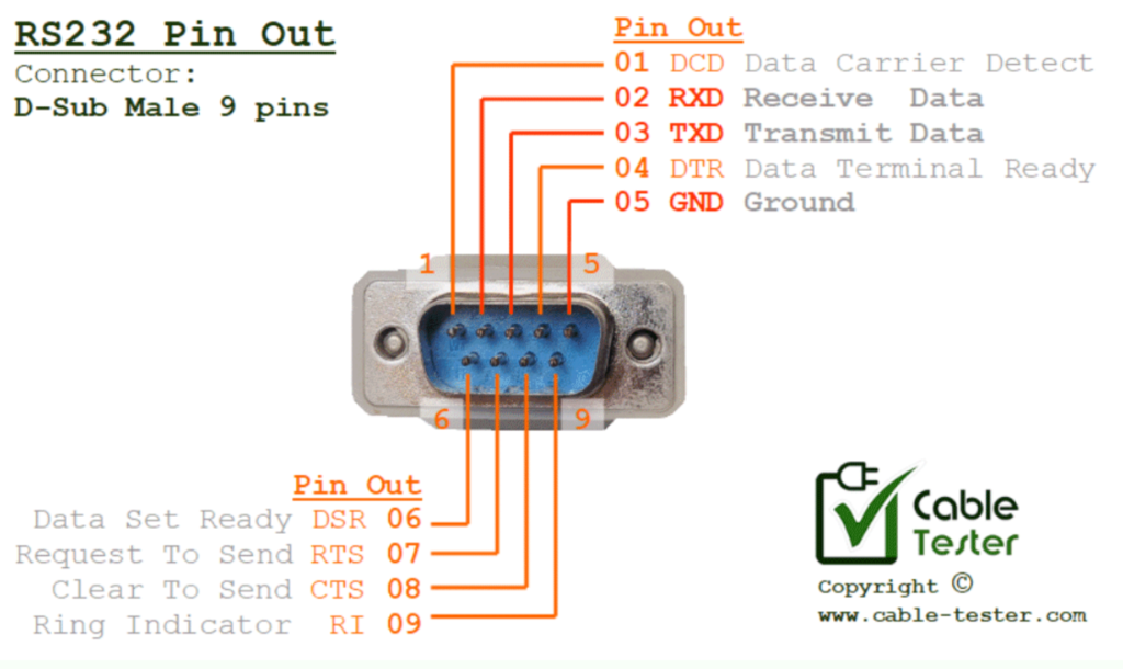
Cable-tester.com has a clearer annotated picture that matches the physical mapping above:
Note that the tutorial itself has Tx(D) and Rx(D) reserved it was building a null modem cable and they skipped all the handshake lines. I’m doing a straight cable (which should be done for internal board header cables where the DB9 socket is male, hence DB9M).
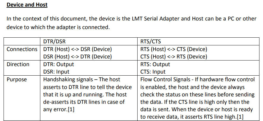
The DTE/DCE might be confusing. Hope these properties can help people make sense out of it (so you can figure it out in your head confidently instead of randomly trying null modem adapters till it work)
- DTE device (colloquially ‘computer’) has the pattern as shown in the pictures above (receive pins above/before the transmit pins), which is usually the computer end and the port/socket is male. Think of it as the ‘driver/master’ (though it’s arbitrary)
- DCE device (colloquially ‘modem’) reverses all the sends and receives of the DTE. Can think of it as the ‘receiver/slave’ (though it’s arbitrary). It’s usually the modem and the port/socket is female.
- For DTE-DTE (like data transfer between two PCs), the send lines on one side should go to the receive lines on the other side. A null modem cable that swaps the send pins with receive pins. You can think of it as making one side DCE. Given that the topology is symmetric, it’s up to the software set up to decide which side is the initiator/client (master) and which side is the reactor/server (slave)
- The handshaking (optional) and flow control (optional) lines also have their initiator/reactor roles reversed with null modem cable.
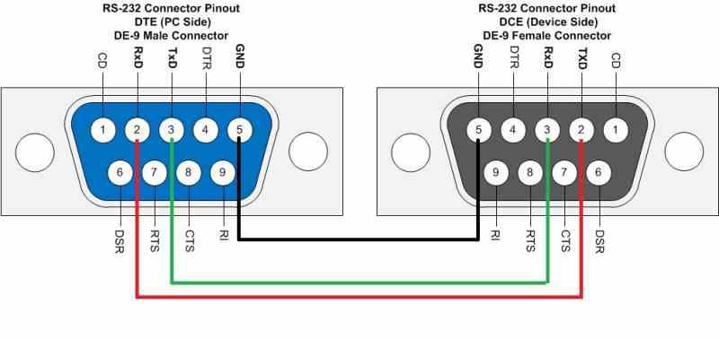
Here’s an image for the above mapping:
It turns out the direct geometric mapping (IDC male pins match the relative locations of the DB9 male pins) mentioned above is the less common type of motherboard header configuration. IDC ribbon crimp-on DB9 headers like this:
![ฅนบ้ายอ: [34+] Db9 Male And Female Connector Pinout](https://external-content.duckduckgo.com/iu/?u=https%3A%2F%2Fsharvielectronics.com%2Fwp-content%2Fuploads%2F2020%2F09%2FD-SUB-DB9-9-Pin-Male-Connector-To-IDC-Female-10-Pin-Flat-Cable-30CM_1.jpg&f=1&nofb=1)
has to follow the above geometric layout since the pins cannot be remapped (so it has to follow the ribbon order). The soldered version looks like this:
However, the more commonly seen soldered RS-232M to IDC10 header uses a transposed configuration (which DB-9M pin numbers matches IDC-10 pin numbering EXACTLY despite one is row-major and the other is column-major), which has nothing to do with the IDC10 pin layout mentioned above.
(I don’t think it’s a good idea to call it ‘crossed-config’ like CWC did.
It almost mislead me to think it happens to swap the roles of Tx and Rx.
I did the mapping on paper and it didn’t make any sense.
Let’s call it ‘transposed-configuration’)
The crazy thing about the existence of these 2 pin layouts is that there’s no easy way to tell which pin layout/mapping it is until you open the connector up and inspect the solder joints! Taking a pin and probe it with a multimeter is more work than taking the screw posts out and disassemble the connector.
So if you just buy some old scrap parts that came with old motherboards, this might confuse the heck out of you until you tested the pin mapping with a multimeter and realize things doesn’t add up!
Note to self: just open the DB9 side up whenever I see a DB9-IDC cable and mark the configuration on the DB9 end directly on the cable!
![]()