If you’ve programmed in (or studied) C++ long enough, like you have read Scott Meyers’s Effective C++, which is a book organized in, jokingly, commandments like ‘thou shall make destructors virtual’. There’s a lot of stuff to remember.
I’ve found an approach to make the ideas stick: by understanding the rationale behind these commandments through the lens of ‘What would you do if you were to make C++ (features) out of C?‘
C++ is not a language designed from scratch. A lot of quirks and oddities in C++ came straight from the philosophy and the language features naturally available in C. With the right jargons (concepts), you will find a lot of the seemingly counter-intuitive behavior ‘it ought to be like this because of (insert design choice here)‘.
This is what we are going to explore in the “Rational Behind C++ Commandments” (RBCC) blog post series which came from my notes when I was going through Scott Meyer’s book. Once you get the ideas, you should be able to come up with the rules in Effective C on your own (so you don’t have to blindly remember them).
Dart’s documentation at the time of writing (2021-10-27) is not as detailed as I hoped for so I don’t know if the Lambda (anonymous function) is late-binding or early-binding.
Free symbols (relevant variables in outer workspace)
bound/captured at creation (no free symbols)
left untouched until evaluated/executed (has free symbols)
Snapshot
during creation
during execution
Late-binding is almost a always a gotcha as it’s not natural. Makes great Python interview problems since the combination of ‘everything is a reference‘ and ‘reference to unnamed objects‘ spells trouble with lazy evaluation.
I’d say unlike MATLAB, which has a more mature thinking that is not willing to trade a slow-but-right program for a fast-but-wrong program, Python tries to squeeze all the new cool conceptual gadgets without worrying about how to avoid certain toxic combinations.
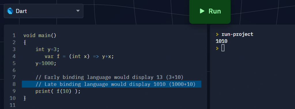
I wrote a small program to find out Dart’s lambda is late-bound just like Python:
void main()
{
  int y=3;
    var f = (int x) => y+x;
    // can also write it as
    // f(int x) => y+x;
  y=1000;

  print( f(10) );
}
The result showed 1010, which means Dart use open lambdas (late-binding)
Language
Binding rules for lambda (anonymous functions)
Dart
Late binding Need partial application (discussed below) to enforce early binding.
Python
Late binding. Can capture (bind early) by endowing running (free) variables (symbols) with defaults based on workspace variables
C++11
Early binding (no access to caller workspace variables not captured within the lambda)
MATLAB
Early binding (universal snapshot, like [=] capture with C++11 lambdas)
I tried to see if there’s a ‘capture’ syntax in Dart like in C+11 but I couldn’t find any.
I also tried to see if I can endow a free symbol with a default (using an outer workspace variable) in Dart, but the answer is no because unlike Python, default value expressions are required to be constexpr (literals or variables that cannot change during runtime) in Dart.
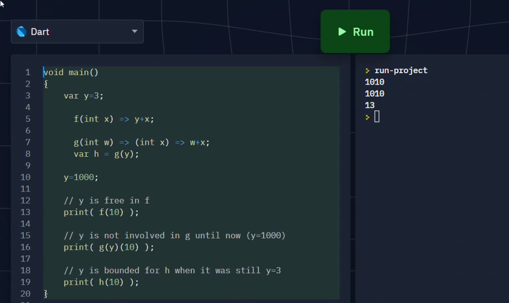
So far the only way to do early binding is with Partial Application (currying is different: it’s doing partial application of multiple variables by breaking it into a cascade of function compositions when you partially substitute one free variable/symbol at a time):
Add an extra outer function layer (I call it the capture/binder wrapper) putting all free variables you want to bind as input arguments (which shadows the variables names outside the lambda expression if you chose not to rename the parameter variables to avoid conceptual confusion),
then immediately EVALUATE the wrapper with the with the outer workspace variables (free variables) to capture them into the functor (closed lambda, or simply closure) which binder wrapper spits out.
Note I used a different style of lambda syntax in the partial application code example below
void main()
{
  var y=3;
    f(int x) => y+x;

    // Partial Application
    g(int w) => (int x) => w+x;
    // Meat: EVALUATING g() AT y saves the content of y in h()
    var h = g(y);

  y=1000;

  // y is free in f
  print( f(10) );

  // y is not involved in g until now (y=1000)
  print( g(y)(10) );

  // y is bounded for h when it was still y=3
  print( h(10) );
}
Only h() captures y when it’s still 3. The snapshot won’t happen if you cascade it with other lambda (since the y remains free as they show up in the lambda expression).
You MUST evaluate it at y at the instance you want y captured. In other words, you can defer capturing y until later points in your code, though most likely you’d want to do it right after the lambda expression was declared.
As a side note, I could have used ‘y’ instead of ‘w’ as parameter in the partial application statement
g(int y) => (int x) => y + x
but the ‘y‘ inside g() has shadowed (no longer refers to) the ‘y‘ in the outer workspace!
What makes it confusing here is that quite a few authors think it’s helpful (mnemonics-wise) to use the free variable (outer scope) name you are going to inject into the dummy (argument) as the name of the dummy! This gives the false impression of the variable being free while it’s bounded (through feeding it as a parameter in the wrapper/outer function)!
Scoping rules is a nasty source of confusion in understanding lambda calculus so I decide to give it a different name ‘w‘. I’m generally dismissive of shadowing under any circumstances, to the extent that I find Python’s @ syntactic sugar for decorators shadowing the underlying function which could have been reused somewhere (because it’s implicitly doing f=g(f) instead doing h=g(f). I hate it when you see the function with name f then f was repurposed to not mean the definition of f you saw right below but you have to keep in mind that it’s actually a g(f)). See my rants here.
Notational ambiguity, even if resolvable, is NOT helpful at all here especially when there are so many level of abstractions squeezed into so few symbols! People jumping into learning the subject quickly for the first time should not have unnecessarily keep track of the obscure scoping rules in their head to resolve the ambiguities!
Complex expressions in lambda calculus notation here is hard to parse in the head correctly until the day I started using Dart Language and noticed the connection between => lambda notation and C-style function layout. Here’s what I learned:
The expressions are right-associative because the right-most expression is the deepest nested function
Function application (feeding values to the arguments) always starts from left-to-right because you can only gain entry to a nest of functions starting from the outermost level, peeling it layer by later like an onion. So if applying arg to statement is denoted by (statement arg), the order of input would be (((statement arg1) arg2) arg3)
Names showing up on the parameter list of the nearest layer sticks to it (local to the function) and excludes everybody else (variable shadowing): this means the same name have absolutely no bearing as a free variable or being a free variable anywhere, so you can (and should) replace it with a unique name.
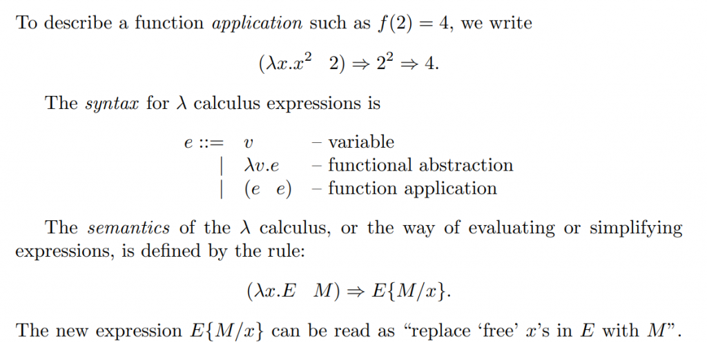
Here’s the calculus syntax in the book:
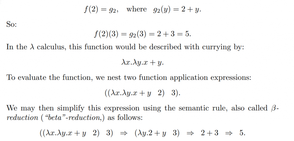
This example is the function application used above
Here’s where reusing the variable in multiple places to mean different things gets confusing as hell, and the author (as well as the nomenclature) do not emphasize the equivalence to variable shadowing rules:
This can be rewritten as having
Upon application,
which clearly reads for an input of , it’ll be incremented first then squared. Resolving further:
The evils of variable shadowing again! Not only it makes the code hard to read and reason, it also make the mathematics hard to follow!
Use the C++11 style syntax so that it doesn’t look like nested function implementation body instead of a functor nested inside a function:
g(int y) {
  var f = (int x) { return y + x; };
  return f;
}
Note that conceptually what we are doing with the wrapper cascade is indeed nested functions. However, in the wrapper, we spit out a functor (which did most of the partial work) so the user can endow/evaluating it with the last piece of needed info/input:
Official Dart docs is sometimes too simple to provide ultimate answers for various language questions. I discoverd an alternative syntax for named lambda here and here. In Dart,
(args) => expr
is the shorthand for
(args) {
  return expr
}
So the Lambda-style (C++11) names variable by assigning it to a messy functor type (inferred with var in Dart and auto in C++11):
var f = (args) => expr
Which can also be rewritten using C-style function pointer-like declaration except
the body expr is included (which is not allowed in C),
returnmust be explicit in curly braces block.
arrow notation => takes whatever the expr evaluates to (which can be null for statements like print)
it’s simply the function name f in Dart instead of pointer (*f) in C
 in multiple places to mean different things gets confusing as hell, and the author (as well as the nomenclature) do not emphasize the equivalence to variable shadowing rules:
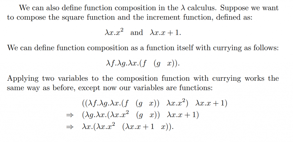


 . It is:
 from the outer workspace (called a free-variable).
  where
where