I was playing around with my TL866 programmer trying to refresh the firmware and needed to get to the recovery mode. However, it seems like the recovery mode info on http://www.autoelectric.cn/en/note.html is incorrect for 2014 design (the one I have). I tried the  as recommended with a decade box and it doesn’t work .
Usually my guess that if somebody is going to set a recovery mode in a micro-controller to be enabled with some hardware path to the power supply rail with a small resistor, it’s just saying that he wants you to pull the pin high.
The said pin is a digital I/O line so I took it as a GPIO pin used for input (I might be wrong)
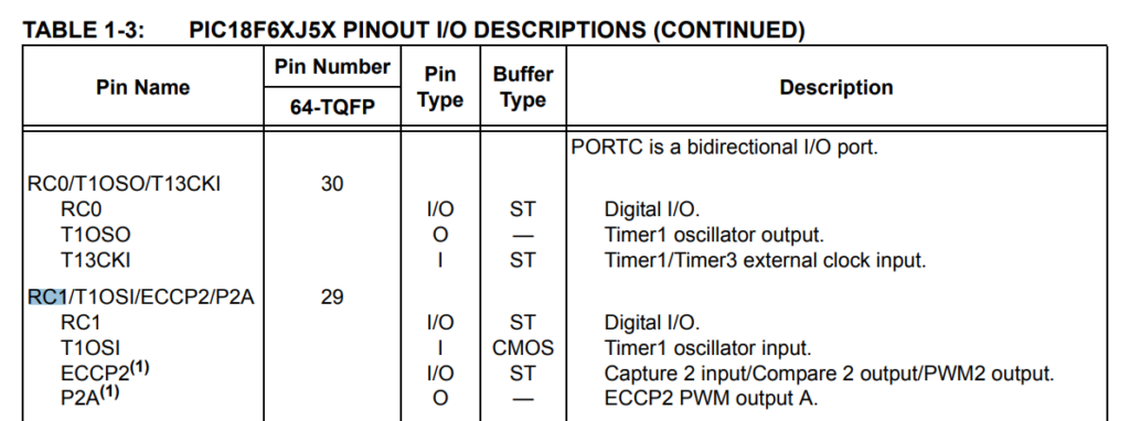
I measured the voltage of the said regulator with a decade box. Interesting that if I flip the resistance while the unit is on, it occasionally remembers the last state when I plug it in again! (EDIT: There is a Schmitt Trigger buffer in between. The buffer type says ST for RC1. Doh!)
Here are some of my measurements with a decade box:
Resistance ( ) ) | Voltage at RC1 in Volts (Pin 29) | State |
| 240 | 0.273 | Autoelectric Recommended |
| 100 | 0.614 | |
| 50 | 1.132 | |
| 45 | 1.246 | Mid-point |
| 40 | 1.358 | |
| 30 | 1.665 | Half rail of 3.3V |
| 20 | 2.157 | |
| 13 | 2.503 | Logic High |
| 3 | 3.041 | |
| 1 | 3.185 | |
| 0 (wire resistance) | 3.191 | Short / Full rail 3.3V |
My guess is that the internal pull-ups config, open-drain changed between versions so the formula to temporarily override (fight) the default resistance that sets the logic level to 0 (basically it’s a tug of war) changed, so the suggested value no longer work consistently.
It puzzles me why a 240 which gives  will be qualified as a logic high by any stretch. Even assuming
  (the supply is
  , but this chip has a internal
  regulator for data lines), sits comfortably in the ‘low for sure’ bin given it’s
  , which is
  . This is how this project got started.
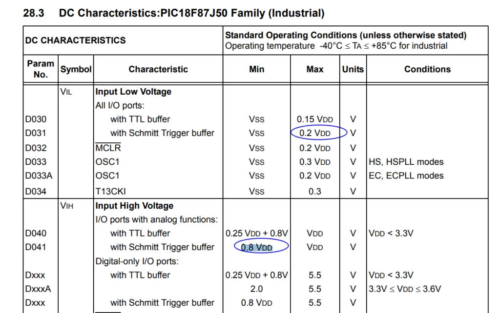 is 0.5V to 2.0V
Given it’s a 3.3V/2.5V capable microcontroller, I’m confident that no manufacturer will design their CPU so that it’d be harmed by forcing a 2.5V logic level line high with 3.3V, and my guess is correct (the digital lines tolerates up to 5.5V).
Just tying the RC1 (Pin 29 where R26 interface with) to the 3.3V rail from the regulator do the trick. No heat-ups, no blow-ups, no malfunctions.
![]()